

Heterostructure Integrated Mirocoolers
With an increasing trend towards miniaturization of electronic, optoelectronic, and micro-electro-mechanical (MEMS) devices, efficient heat removal or thermal design is rapidly becoming an issue of critical importance. For example, fiber optic communications has seen tremendous progress with Tbit/s information transfer capacities for a single fiber. These advances have been possible with the advent of dense wavelength division multiplexing (DWDM). With a wavelength spacing of 25-50 GHz, one needs temperature stability in a typical semiconductor component on the order of 0.1C. While such control is possible with existing thermoelectric (TE) coolers, the cost of optical packages with TE coolers is much higher than uncooled packages, and a cost effective, integrated approach is needed. In addition, most high-speed lasers are limited by thermal effects preventing them from being biased far enough above threshold to get to intrinsic device limits. Recently, we proposed to use thermionic emission in heterostructures to increase the cooling power in conventional semiconductor materials such as AlGaAs, InGaAsP or SiGe beyond what can be achieved with bulk thermoelectrics. Thermionic emission is well understood in semiconductors, and is used in many devices. The hottest electrons are emitted over a barrier and collected on the other side. The coolest electrons remain behind. Consequently, the anode becomes hot, and the cathode becomes cool (see Fig. 1). Theoretical predictions show that HIT coolers can provide 10-40 degrees of cooling per stage. We are currently investigating the following research projects (Fig. 2 and 3):
*Design and characterization of III-V-based superlattice coolers integrated
with long wavelength semiconductor lasers.
*Study of SiGe-based heterostructure devices for integrated cooling of
high power VLSI circuits.
*Experimental investigation of microscale heat generation and thermoelectric
effects in submicron semiconductor devices.
*Study of nonisothermal electron and phonon transport in semiconductors
using Monte Carlo simulation of the Boltzmann equation and the hydrodynamic
model.
Figure 1 Heterostructure Integrated thermionic (HIT) Cooler.
Figure 2 SiGe/Si superlattice cooler structure, TEM image, and measured cooling on top of 50x50 mm2 device for different heat sink temperatures.
Figure 3a 3D simulation of micro refrigerators, SEM picture of devices, and typical characterization using microthermocouples.
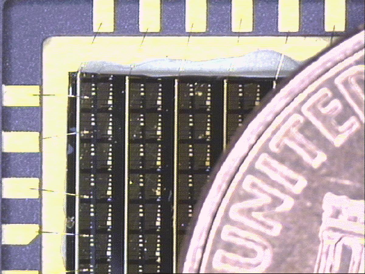
Figure 3b Micro refrigerator
on a chip.
* Thermoelectric cooling in bulk and quantum well semiconductors
* Viewgraphs: Introduction to Thermoelectrics/Thermionics
* Viewgraphs: Novel Micro-TE Coolers
Using III-V Superlattice Structures: Techniques and Possibilities;
Invited Talk, Indium Phosphide and Related Materials (IPRM `02), Stockholm,
Sweden, May 14, 2002.
Graphs
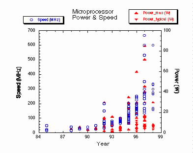
* Microprocessors
speed and power versus year (Tom Burd, UC Berkeley, CPU Info & System
, Performance
Summary)
Submicron Thermal Imaging
Microscope for Integrated Circuits During the period Jan. 2000- September 2000 with the support of the Packard fellowship, and NSF we studied theoretically and experimentally various non-contact methods to measure temperature with sub micron spatial resolution. The technique that seemed most promising was thermoreflectance. The temperature profile is determined by measuring the temperature-induced change in the surface reflectivity. Lock-in technique is needed to detect the small change in the reflectivity (DR/DT~2x10-5 /C). One can generate the thermal image of the device by illuminating the whole surface with a white light source and using a photodiode array for lock-in detection of the thermoreflectance signal at different pixels. Visible wavelength thermoreflectance imaging can give submicron resolution.
To try this method a sample was illuminated with a white light source and excited with current pulses at 200Hz, to allow for heterodyne filtering. The detector was the Hammamatsu 16x16 photodiode array, and several National Instruments data acquisition boards were used for parallel processing of the 256 channels. Dr. Philip Melese at SRI International provided the detector and associated circuitry. Calibration was done using the thermocouple measurements on larger devices. Absolute calibration is difficult because of the uncertainty in the 'thermoreflectance' constant of the surface metal. Future work will be to calibrate absolutely, so that the error introduced by the thermal mass of the thermocouple can be quantified.
Presented are the images of a 30-micron microrefrigerator at 25C. Fig 4 shows a CCD image of the cooler. Surface reflection and interpolated thermal reflectance image are shown in Figs. 5 & 6. Each data point represents a 1Hz bandwidth FFT at the cycling frequency averaged over 20 seconds. We see that there is cooling, but also heating at the junction between the contact layer and the cooler. A cross-section of the thermal image is shown at different currents in Fig. 7. Approximate regions of the contact layer, cooler and substrate are indicated in the figure. The cooling appears to be limited by a large heat load at the junction from contact layer to cooler. By better understanding the cooling distribution, the devices can be optimized to reduce the non-ideal heating effects.
We continue this work in collaboration with Prof. Peyman Milanfar (UCSC) and Dr. Philip Melese (SRI International) in order to improve the spatial and temperature resolution.
Electron Vortices in Submicron semiconductor devices
There has been significant research to include quantum mechanical effects where wave nature of electrons plays an important role in the device operation. There has also been a lot of research on Monte Carlo methods to study the solutions of the Boltzmann transport equation and to consider effects such as velocity overshoot and improved modeling of heat generation in the device. In a recent paper, in collaboration with Dr. Kamran Mohseni at Caltech and Prof. Rajeev Ram at MIT, we analyzed the problem of electron transport in ultra small devices from a hydrodynamic point of view. In analogy with conventional fluid dynamics we derived equations for generation and transport of electron vortices and studied different regimes in which formation of these vortices can have a significant effect on the device operation.
We showed that aside from the conventional stretching term and baroclinic generation of vorticity, there is a source of electron vortices due to the recombination in semiconductor and decay of vortices due to the momentum relaxation. This analysis predicted the conditions for the observation of electron vortices in high field transport in submicron devices.
We continue this work both
theoretically and experimentally by designing novel devices based on electron
vortices and by developing imaging techniques for 2D electron flow visualization.
Injection Current Internally Cooler Light Emitting (ICICLE) Diode
In conventional separate confinement heterostructure LEDs and lasers, the carriers are injected at energies well above the conduction band from a large bandgap material into the small band gap material used as the active region. Since the stimulated emission happens mostly for electrons (holes) that have energy close to the conduction (valence) band minimum (maximum), the injected carriers should relax before emitting photons. This carrier relaxation is a source of additional heat in the active region and it is one of the limitations for high power operation of light emitting devices.
A small bandgap active region is required in order to have light confinement and also this reduces considerably the absorption of emitted light by the larger bandgap contacting layers. Choosing a band diagram under bias, as shown in Fig. 8, combines the advantages of small bandgap active region with injection of carriers near conduction and valance band edges. In addition selective emission of hot electrons and holes above the heterostructure barriers to the active region cools the device. One can get such a band alignment using type II heterostructures. It is also possible to modify the doping profile in the device in order to achieve similar band diagram.
The second law of thermodynamics requires that any cooling (reduction of entropy) in one area should result in heating (increase of entropy) by at least the same amount in another area. However, the increase of entropy does not have to be in the form of heating inside the device. In the above light emitting components, entropy can be generated by incoherent emission of photons that are emitted outside the semiconductor material. In this injection current internally cooled light emitter (ICICLE), upon the current flow, electrons absorb thermal energy from lattice in one region and then they lose their energy in the form of photons that are emitted. This can be viewed as the electronic version of conventional laser cooling which has been used for atom trapping. As it can be seen in Fig. 9, the internal cooling can also be used in unipolar quantum cascade lasers.
Our current emphasis in collaboration with Prof. Rajeev Ram at MIT is on the thermal characterization and modeling of conventional diode lasers and the design of ICICLE diode structures.
Photonic Switching
In fiber optics networks, the transmission has been very successful with commercial 10 Gbit/s time division multiplexed (TDM) and 16-40 wavelengths division multiplexed (WDM) networks and with multi Terabit/s systems demonstrated in various laboratories. As a result, large amounts of data are arriving at switching nodes, swamping the fastest and largest electronic switches. Development of practical optical packet switching systems with low packet loss rate is mitigated by the difficulties to fabricate large size waveguide switches incorporating optical buffers and finding an appropriate synchronization scheme. Extending current wafer fusion technique to integrate various III-V active devices with Si-based waveguides and VLSI can solve many of these problems. In addition of having 3D interconnect topology, one can take advantage of the differences in the materials dispersion in Si, GaAs and InP to realize compact WDM filters, add/drop multiplexers and switches. The packaging of optoelectronic devices with single mode fibers can also be facilitated by the use of large diameter and low loss Si-based waveguides and V-grooves. We are currently investigating the following research projects in collaboration with the Center for Multidisciplinary Optical Switching Technology (MOST) at University of California at Santa Barbara:
*Design of tunable couplers and add/drop multiplexers based on fused InP/GaAs
waveguides.
*Integration of 1.55 µm semiconductor optical amplifiers with silicon
photonic integrated circuits.
Graphs
* Telecommunication data rates versus year (Howard Banks, "Life at 100 billion bits per second", Forbes Magazine, Oct. 6, 1997)
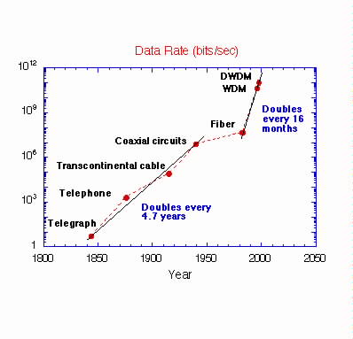
* Number of
Internet hosts and networks versus year (Robert H'obbes' Zakon ,
Hobbes' Internet Timeline
v3.3)
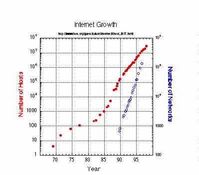
![]()